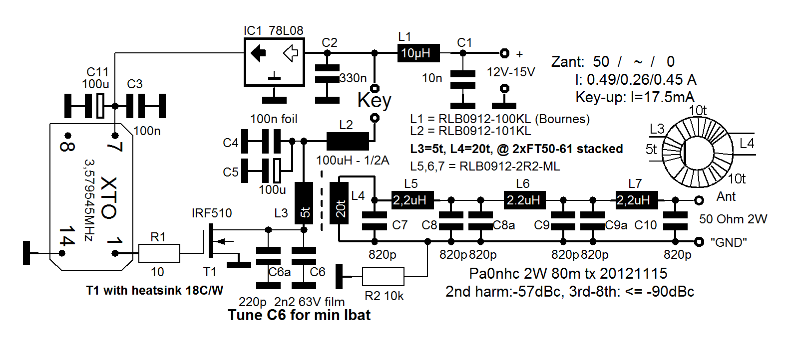
The pa0nhc 2W, CW or AM ARDFtx for 80m.
(20121115) 20130504 PDF added / 20150123 layout.
To print a picture, click on "PDF"
Print PCBmasks as "100%" or "In original dimensions".
Properties:
- Optimally designed for superCLEAN output at 3.579545 MHz.
2nd harm -57dBc, 3rd - 8th <= -80dBc !
No seeping-through of digital spikes !
- Rugged output stage
can withstand severe mismatch from open to shorted output connection.
No transmitter damage if antenna becomes damaged
No parasitic oscillations.
The output stage is keyed or modulated.
Small keying bandwidth: a few kHz.
- Needs only 1/2A from a 12.6V battery for 2.5W output.
Can work up to 4 hrs from a 1Ah battery when in CW operated ARDFmode (1min on, 4min off)..
- Uses a cheap, standard XTO as oscillator/driver.
No tuning, always exactly on correct frequency
Reliably starting, ample drive.
- Filter coils are standard available mini inductors
Only one ferrite ringcore (output transformer) must be wound.
- Easy first setup:
Simply tune ONCE for minimum supply current on a dummy load with key-down, and check current and output.
Ready.
- Fast setup in field circumstances.
Just connect and tune the antenna.
Ready.
- Single sided PCB for readily available through-hole components
Small size: 50.8 x75.184 mm2. It will fit inside a 60mm PVC pipe.
Simple. Easy to build. No SMD parts.
- FET and the cooling fin are directly mounted on the insulated top of the PCB
No extra insulation needed.
|
Componentlist |
|
| XTO 3.579545MHz (Dil14) | 1 |
| Foil C 220p 100V | 1 |
| Cer.C NP0 820p | 6 |
| Foil C 2n2 100V | 1 |
| Cer.C 10n | 1 |
| Cer.C 100n | 1 |
| Foil C 100n 65V | 1 |
| Cer.C 330n | 1 |
| Elco 100uF RM2.5 | 2 |
| Inductor 2.2uH RM5 | 3 |
| Insulated wire 0.7mm dia | 1m |
| Inductor 10uH RM5 | 1 |
| Inductor 100uH RM5 | 1 |
| Ferrite toroid FT50-61 | 2 |
| Resistor 10 Ohm RM10 | 1 |
| Resistor 10kOhm RM10 | 1 |
| IRF510 (TO220-AB package) | 1 |
| Heath sink for TO220 land | 1 |
| 78L08 | 1 |
| PCB screw connector 2-pole | 3 |
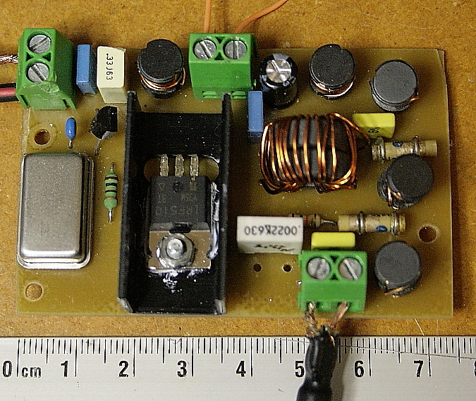
(This prototype differs slightly from the actual PCB).
The output transformer is wound onto two stacked toroids FT50-61.
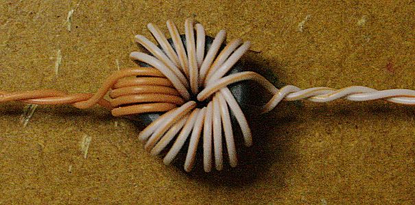
Windings L3 (left) and L4 (right). Used wire: stripped from CAT5 cable.
If available, use a bit thinner, plastic insulated wire for L4.
Valid for every toroide:
Each time a wire passes the toroids hole, it counts as one full turn.
Try to keep the windings flat against the body of the toroids.
How to:
Glue two FT50-61 toroids with the sides onto each other, using 10s glue.
Best use Teflon (R) insulated wire.
First wind L3 (here orange, 5x through the hole).
Twist the ends firmly until the turns are close to the toroid.
Straighten the wire for L4, and fold it double.
The begin and the end of L4 must be near each other.
See schematic diagram and photo. Wind as follows:
Wind the first half of L4.
10x through the hole, starting closely against L3.
The remaining wire half, first has to go diagonally through the hole.
Then wind it onto the opposit side of the toroid, starting against L3.
Pass it in total 10x through the hole.
Twist the wire ends of L4 until the last turns are close to the toriode.
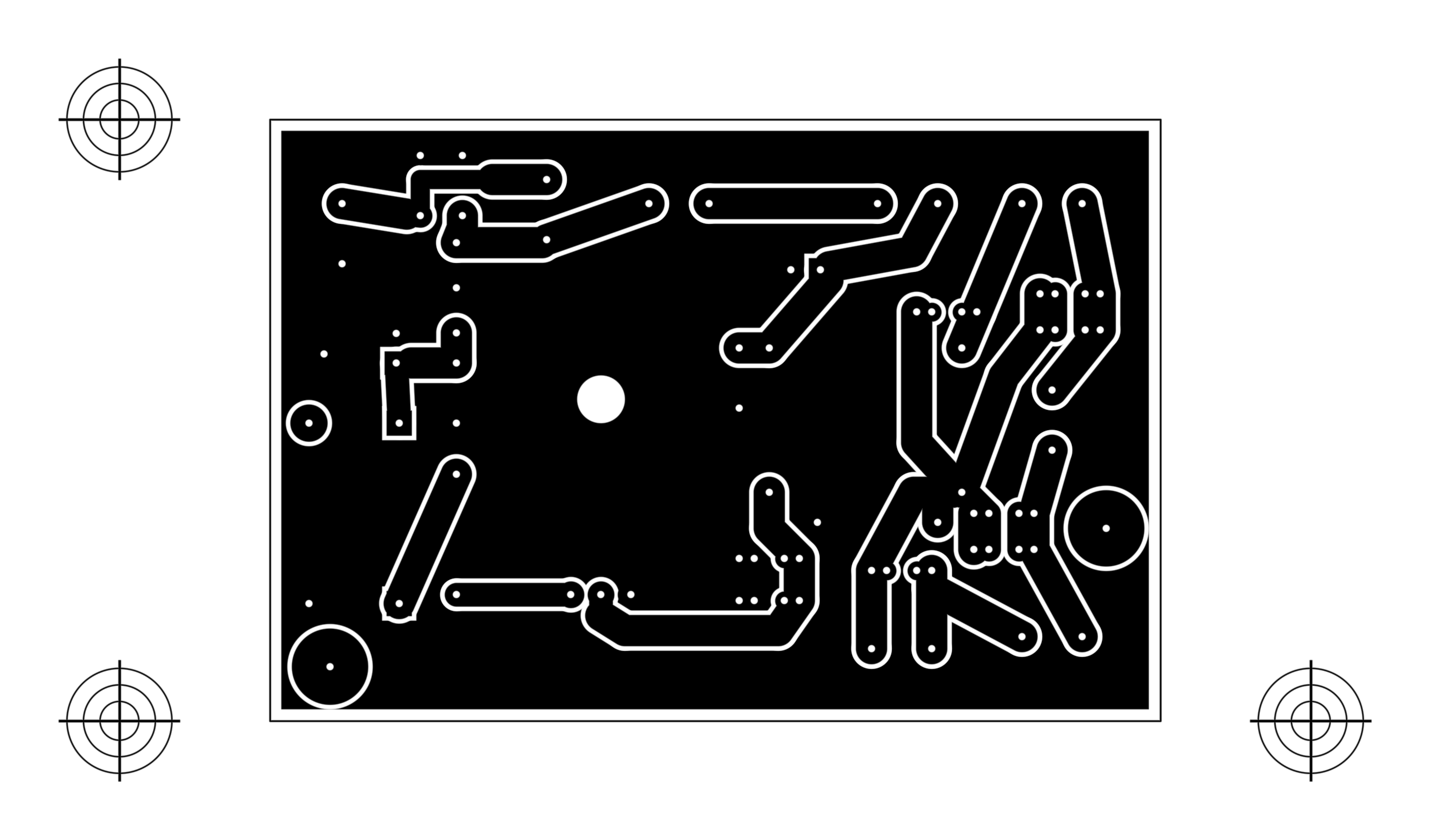
Bottom copper mask (600DPI) seen from top.
PDF
S1, S2 and S3 are 3.25mm holes for mounting.
(This layout differs from the shown prototype)
PDF
Observe: The connections of TO220-AB differ from TO220-I.
Keep this in mind when using another type FET.
Drain waveform (10V/div, +70 / -10V) when L3 is correctly tuned and loaded.
Drive voltage from XTO to the IRF510 (2v/div, +14 / -2V) when L3 is correctly tuned and loaded.
Setup, tuning.
ADVISE: allways use a 1A fuse in the battery line ! Danger of fire !
If the XTO should become demaged, and its output voltage staying HIGH, the FET becomes to hot, and immediately burns out !
You can "pre-tune" L3 rawly :
- Disconnect battery and antenna
- Change C6 until a dipmeter shows that L3 is resonating around 3.8MHz (yes: three point eight Megahertz).
After that, definitive tuning must be done as follows by observing the battery current:
1. Connect a dummy load, wattmeter and 12.6V power through a amperemeter (10A range).
2. With key down for a short peroid, observe the battery current and outputpower.
3. Change C6a, and repeat 1-2-3 until the battery current is minimal (ca. 0.5A), while the output is ca. 2.5W.
4. Then (if possible) check the level of the 2nd harmonic (ca. -57dBc).
After i tuned this way, a check with a dipmeter (power and antenna disconnected) showed a resonance of L3/C6 at 3.8MHz. NB: two other resonances at 4.4MHz and 5.2Mhz are probably in the PI filter or L2. Do not bother.
Resulting currents and temperatures:
- At key-up the battery current was only 17.5mA. Fundamental output was -50dBc.
- At key down, loaded with 50 Ohms, the battery current was 0.49A, and the output was 2.5W.
The dissipation then is (0.49A x 12.6V) - 2.5W = 3.7W.
The temp. rise of the cooling fin can be calculated to 18C/W x 3.7W = 67C.
The temp of the internal FET then is ca. 100C. As the max. temp of the FET is 175C, it is in a safe region.
- Unloaded (with open antenna connection) and key-down, the battery current was 0.26A.
Dissipation 3.3W.
Temp rise will be abt. 60C.
- With a shorted antenna connection and key-down, the battery current was 0.45A.
The temp rise will be 102C.
Not recommended for a long period. But a shorted antenna cable during a foxhunt will not damage the transmitter.
If this transmitter should operate continuesly, care must be taken for good airflow or a bigger cooling fin.
Devellopment history :
Several prototypes of a 3.5MHz 2W transmitter were made and tested.
The first with XTO, 74HC240 driver and one VN88AFD powerfet, and a wideband output transformer, had only -40dBc 2nd harmonic suppression.
Someone suggested: use a balanced output stage to suppress the 7MHz harmonic.
Several balanced versions were made. After tuning the primairy of the output transformer to the carrier frequency, it resulted in -60dBc 2nd harmonic
and 2W fundamental output. Nice? But:
- the efficiency was worse
- the PCB was larger
- the output tranformer more difficult to make (bifilar primairy)
- and it costed extra parts
Moreover, when the drain waveforms were observed, a lot of "ringing" was seen. This is probably the result of suddenly changing parasitic resonances in the FET output circuitry, when drain voltages (and thus the FETs output capacitances) varied much. With small gaps inbetween when one outputFET was taking-over from the other. This could lead to radiation of non-harmonic spouriï.
That first design with only one FET was therefor modified and simplified. Now using a tuned tank circuit. The 74HC240 driver was
omitted.
After correctly tuning L3, the output from the XTO was good enough to drive the powerFET.
The VN88AFD FET was not commercially available anymore, so it was changed to a very cheap IRF510. This is a powerfet with not to high in- and output capacitances, and low saturation voltage.
The ouput PIfilter was enlarged with one section for more 2nd harmonic suppression.
In a PCB containing a mix of digital and HF cicuits, the purity of the output power stands or falls with the layout of the PCB.
Much attention therefor now was payd to the PCB design:
- The various retour-paths in the "mass"plane are short, lowZ and do not cross.
- The entire output cicuit (trafo-sec / PIfilter / Ant connector) is completely insulated from the mass plane and the rest of the circuit (exept for a hi-Z static voltage
leakage resistnace).
This prevents that digital needle- pulse- currents and harmonics, running in the "0" mass plane (from the XTO and the FET), could be coupled into the "GND" return path of the output circuit.
A tuned output transformer prooved to be important too:
- it helps to suppress 2nd and higher order harmonic output
- it improoves efficiency
- and it reduces the need for more drivepower.
Tuning variations in this circuit still have a profound influence onto the drain waveform, to the battery current and to the gate-drive-waveform.
The gate drive waveform changes with varying drain load, due to the rather large drain-to-gate feedback capacitance.
With varying drain-to-source voltages, the output capacitance of the IRF510 powerFET varies between 300pF and 60pF (!). Consequently, the resonant frequency of the output circuit varies largely with key-up and key-down (no drain current / high drain current and high drain voltage / low voltage).
Defintive tuning of the output circuit for resonace with the use of a dipper is therefor not recommended. The circuit will then be out-of-tune when keyed.
Correctly tuned, the drain waveform peak values were -2 to +35V (see photo), and battery current was minimal.
The battery current can be measured easiest. Thus:
Tune L3 definitive for MINIMUM battery current, while "Ant" is loaded with 50 ohms.
Simple and effective.
Success es 73's, Nico.