 |
 |
|
Pa0nhc 3.579545MHz 66mW MiniTx "Sputnik". |
This very small transmitter (only 34mm x 41mm) is developed after a raw idea from the ARRL.
It can operate from a 9V or 6V battery.
|
|
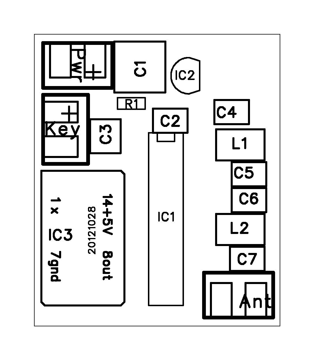
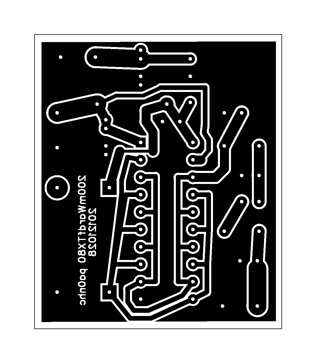
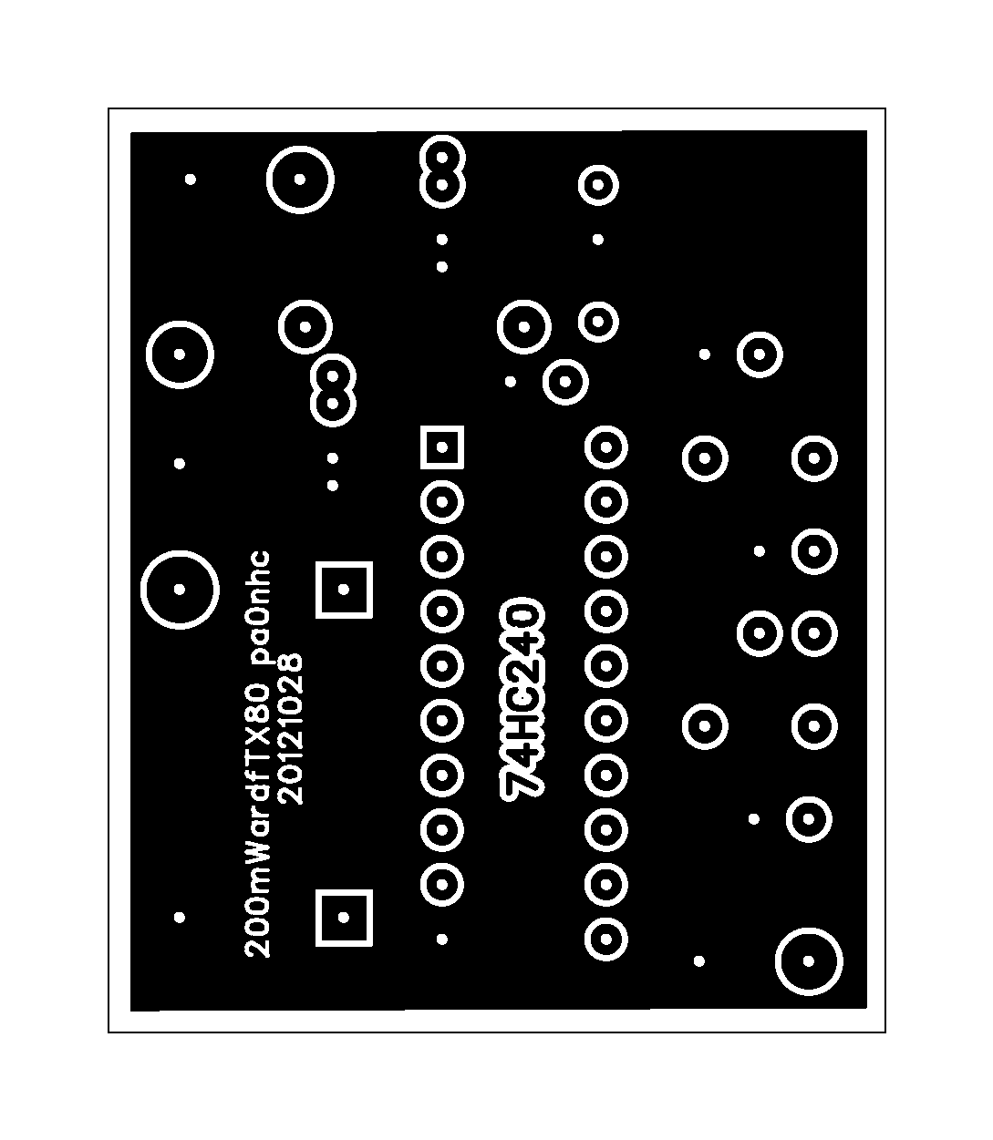
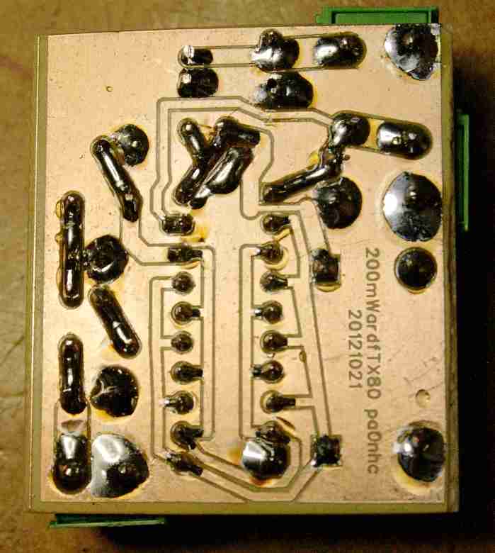
Double sided PCB for clean signal.
WARNING:
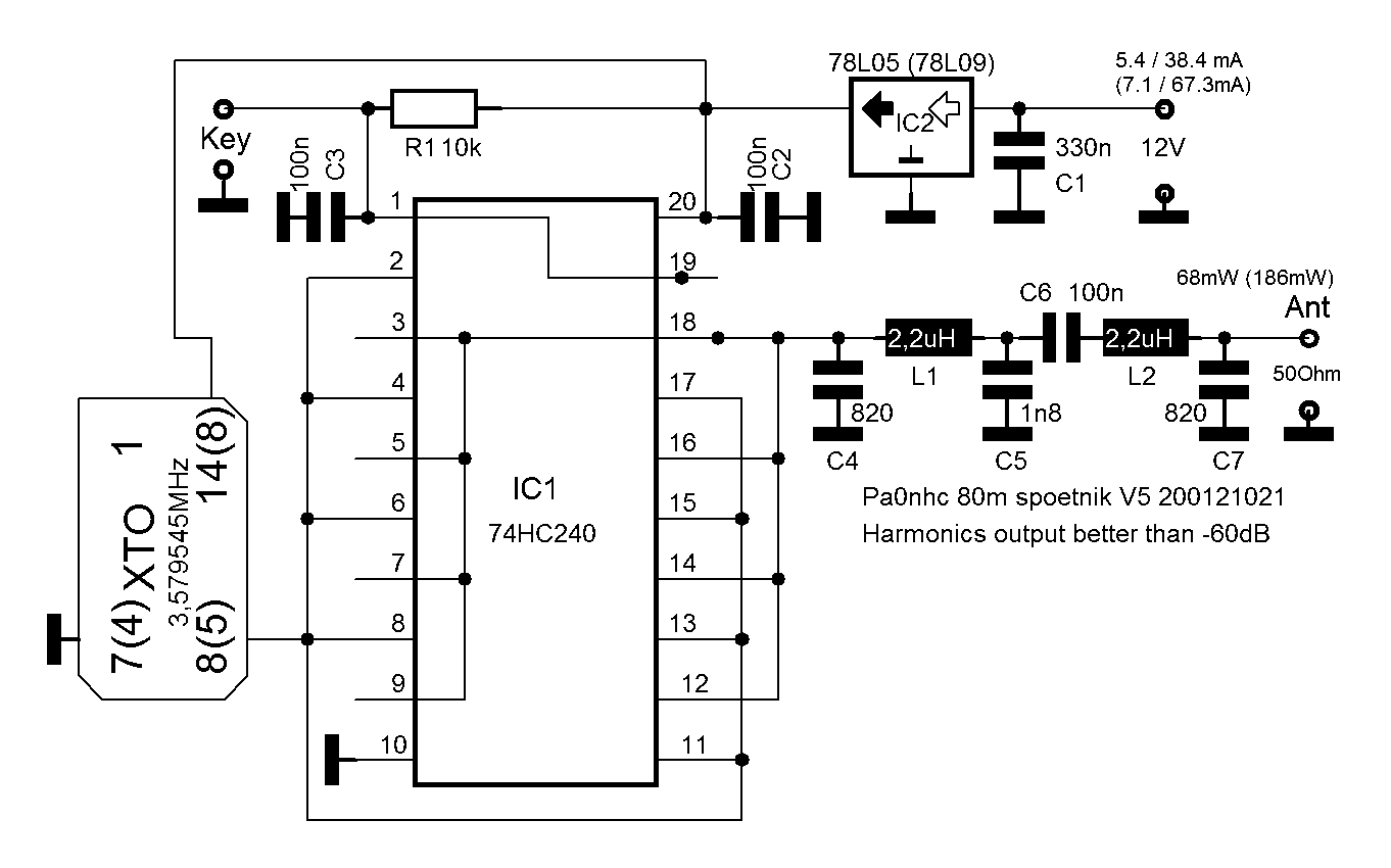
The oscillator of this little transmitter is always "on". Keying (switching on/off) is done by simply connecting/disconnecting the enable inputs of IC1 to "GND".
IC1 will switch the carrier on and off with very short rise- and fall times (nanoseconds) .
This simplest way of keying WILL result in clicks wich occupy MHZs wide bandwidth !!
Do NOT use this little transmitter as a driver preceding a power amplifier !!
When only this low 66mW power is fed into a short ARDF antenna with very poor efficiency, it will have at most a few hundreds meters ground wave range. The interference will be small and unnoticeable for non-fox hunters further away.
|
Do NOT connect this circuit to a poweramplifier, which in turn is connected to a high efficiency antenna system.
Especially NOT when modulating with digital signals. You WILL saturate a wide frequency range with clicks, rattle or "bleeps". |
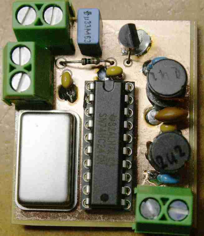
Details.
This little transmitter can be operated from 5V to 12V, or directly from a 9V battery.
It makes 66mW output (with a 78L05) to max. 200mW output (when powered via a series diode from a 9V battery) into 50 Ohms load on a fixed frequency in the 80m band.
It could be used on higher amateur bands too (not tested). The TXO and the output low pass filter must then be adapted to the used frequency.
IC2 switches the carrier frequency ON/OFF in nanoseconds. In decoupling capacitor C3 are running the nanosecond short, but relative strong needle-pulse currents from the carrier frequency. These pulses run from pin1 back to pin10.
To prevent voltage losses in the return path through the mass plane, that path must be as short and wide as possible, and strictly separated from the rest (output) of the circuit. If these currents could couple (crossing paths) with other circuits, unwanted harmonics should directly be coupled into the antenna.
| Only with the double sided PCB design shown here, all harmonics will be weaker than -60dBc. |
This double sided PCB was carefully developed with a separate, short, lowZ retour path for the decoupling circuit of the IC, and a separate return path for the filtered output signal. Observe the "isolating tracks" in the PCB.The measurements were done to this double sided version.
No SMD components were used for easier assembly. If connections to power, key and ant. will be made by soldering wires, the three PCB connector blocks are left out.
All mass connections of IC1, IC2, C2, C4, C5 and C7 should be soldered at both PCB sides. This makes all signal retour paths as lowZ as possible, resulting in the cleanest output.
REM : In order to be reachable with the soldering iron tip, these components must then be lifted abt. one millimeter at the mass connection. Solder them on the top copper side FIRST.
Only the fundamental frequency passes the double PI output filter to the antenna connector. C6 blocks the DC component, so it cannot be shorted to "GND" by the antenna. Use NP0 capacitors or film capacitors here.
Despite of the simple low pass filter, the 2nd harmonic is already weaker than -60dBc. The symmetrical square wave output of the XTO unit is accountable for that good result.
With a non-symmetrical output from a discrete Xtal oscillator or VFO, this result is probably not
possible.
So stick to the use of a cheap XTO.
The XTO drives all eigth inputs of the "power amplifier" IC1 in parallel. The paralleled output waveform of IC1 still is a symmetrical square wave. Therefore all even harmonics are weakened naturedly. The 3rd harmonic is easier blocked by a simpler low pass filter than the 2nd, as it is farther away from the fundamental frequency. A clever simple way to get clean output.
|
|
|||
|
Click-right on a picture to download it.
Print the mask "Size 100%" or "With original dimensions".
The transmitter was tested and measured in versions with for IC2 an 78L05, and a TO220 type 7808. The 7808 stabilizer was fed from 12V. Due to the higher current drawn it dissipates to much to be an L type.
Currents drawn (key-up / key-down):
with 78L05 : 5.4 / 38.4 mA.
With 7808 : 7.1 / 67.3 mA.
This mini transmitter can also be operated directly from a 9V battery. Then exchange IC2 for a SI diode (1N4148). The diode lowers the supply voltage to abt. 8V, and prevents for damage bij wrong polarization of a battery. Operation time is then estimated to 3hrs. NB: during a test this worked, but the IC's are "streched to the limit".
L1 and L2 are readily available mini inductors, and can be rectangular or round.
In the tested PCB, all capacitors except C1, were ceramic types, 5%. As foxhunt transmitters can be used in very low and very high surrounding temperatures, C4 to C7 should be NP0 type.
IC1 was soldered directly into the PCB with a drop heath paste under it for direct cooling through its body and legs.