|
|
|||||||||||||||
|
|||||||||||||||
|
|
| << |
Assembling and installing a
PCB.
|
(C)
The use, copy and modification of all info on this site is only permitted for non-commercial
purposes, and
thereby explicitly mentioning my radio amateur call sign "pa0nhc" as
the original writer / designer / photographer / publisher.
|
|
|||||||||||||||
|
|||||||||||||||
|
|
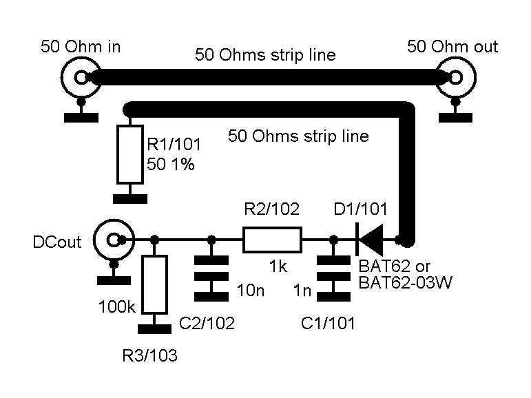
Assembling and installing a PCB (see schematic and parts List ==>).
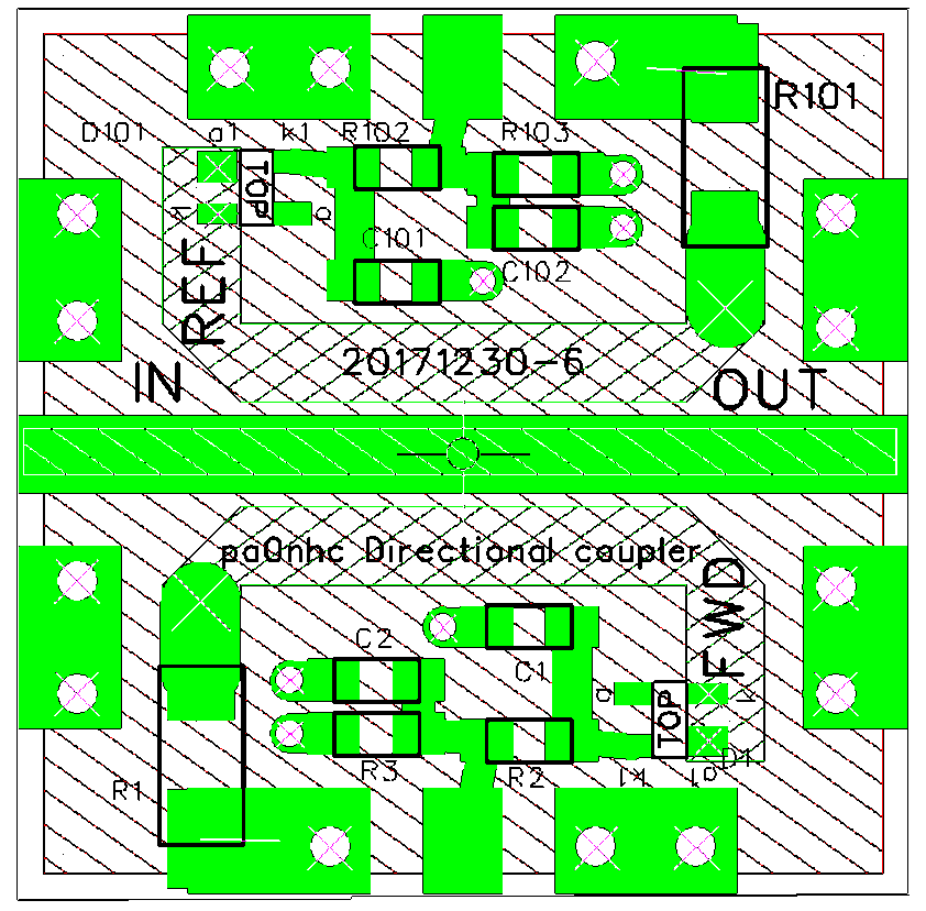
On the DC type PCB's, all component designators are printed. Simply solder there the components from the parts list.
|
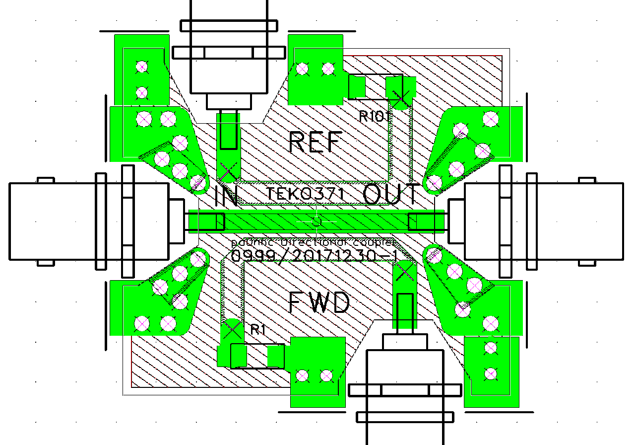
Prevent static damage to semi conductors. Before installing the BNC
busses in the box,
put the PCB in the enclosure first. The PCB will be installed with the top copper surface against the underside of the BNC pins. The BNC ground lugs must be soldered onto the PCB top copper. The
PCB upper mass surfaces must ONLY make contact to the BNC grounfing
lugs, NOT to the inside of the box. |
After installing the BNC busses,
- Solder the BNC pins to the PCB traces at the PCB top
surface.
- Solder both ground lugs of each BNC bus to the grounding
surfaces on the top surface of the PCB.
The PCB mass planes must only be connected to the box with two ground lugs at each BNC bus.
For high power uses (more than 400W), the current capacity of the through line track needs to be improved. It can be filled with a thicker layer of solder tin. This track intentionally is partly kept free from solder mask.
Test.
At 145 MHz, the FWD port of the RF couplers should show -32dB output, whith
all outputs terminated with good terminating resistors.
REM : the actual output of the REFLected ports depends on the tolerance
of the 50 Ohms terminating resistors !
If a measurement output is to high, check the terminating resistor.
REM : Best accuracy could be obtained, by
using an RFcoupler in combination with very accurate RMS RF detectors :
AD8361ARTZ.
See : pa0nhc RF watt meter 20170808 v18
DC coupler output :
The following values are only an indication what can be expected, with the
forward port loaded with
1Mohm or higher value.
According to BAT62 data, at 145 MHz the output should be :
- with 1,57W RF input, the output ia abt. 0.09
Vdc.
- with 100W RF input, the output is abt 1.79 Vdc,
- with 800W RF input, the output is abt 7.16 Vdc.
Parts.
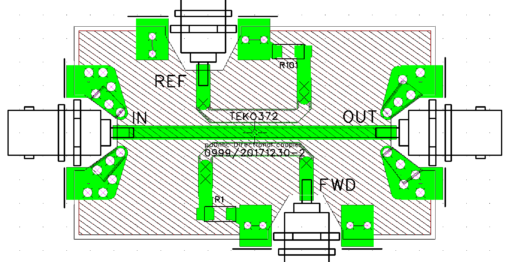
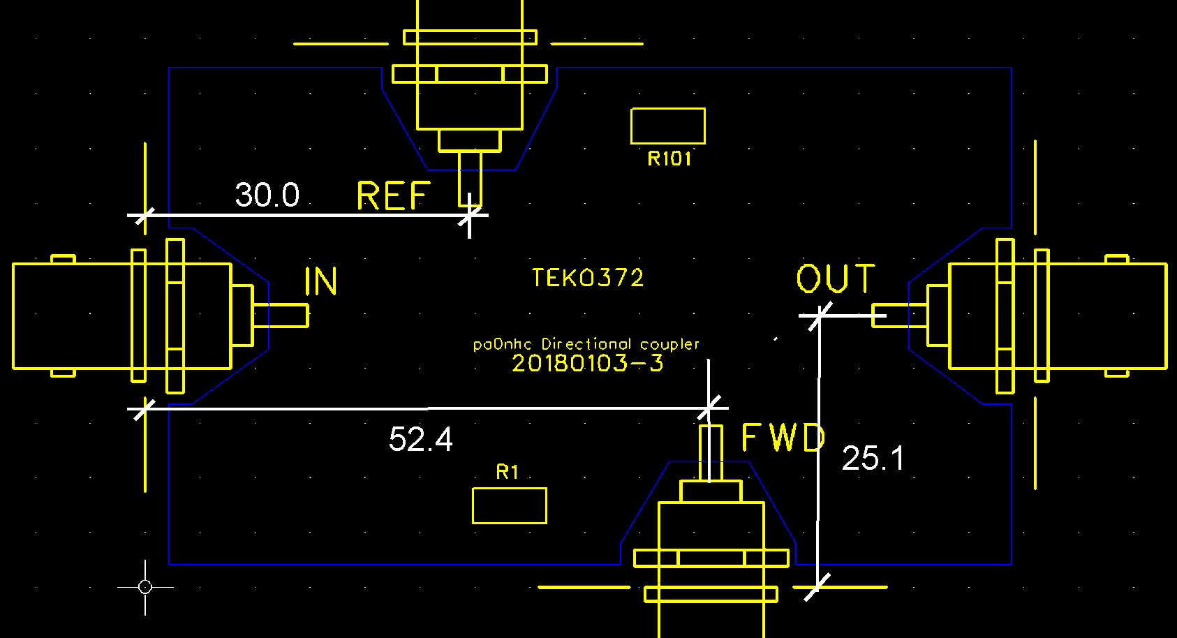
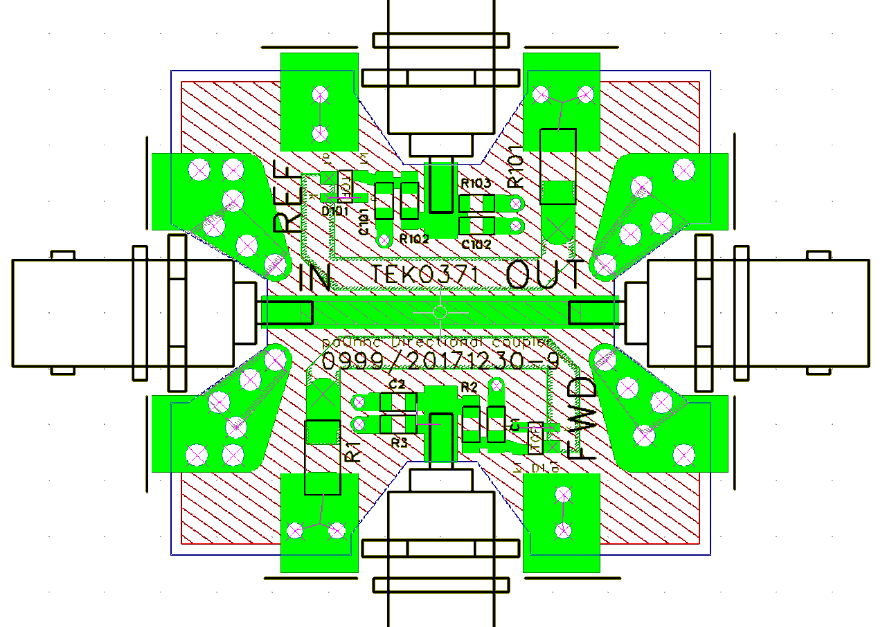
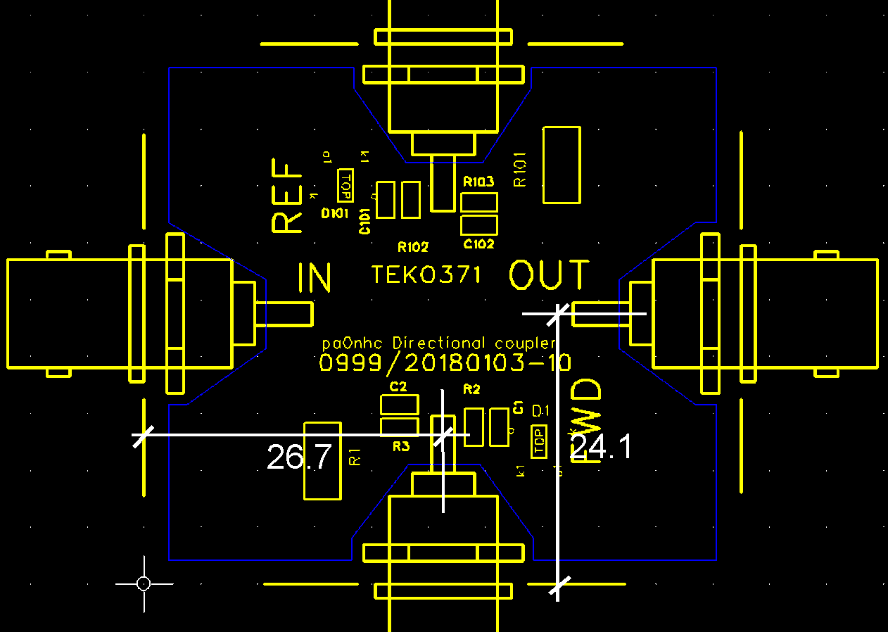
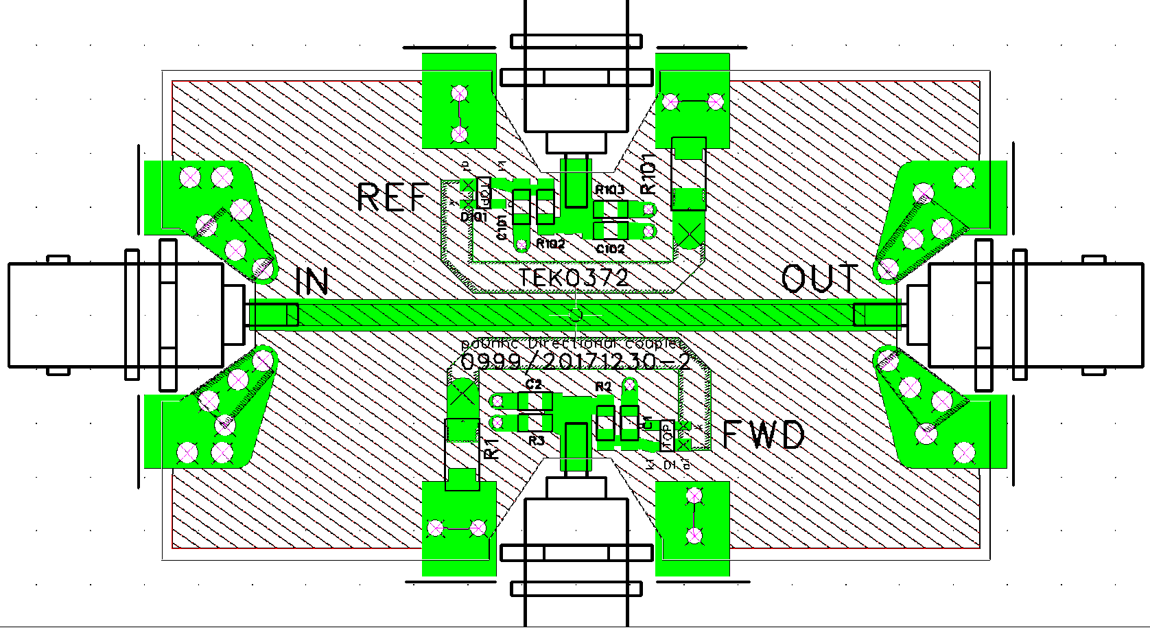
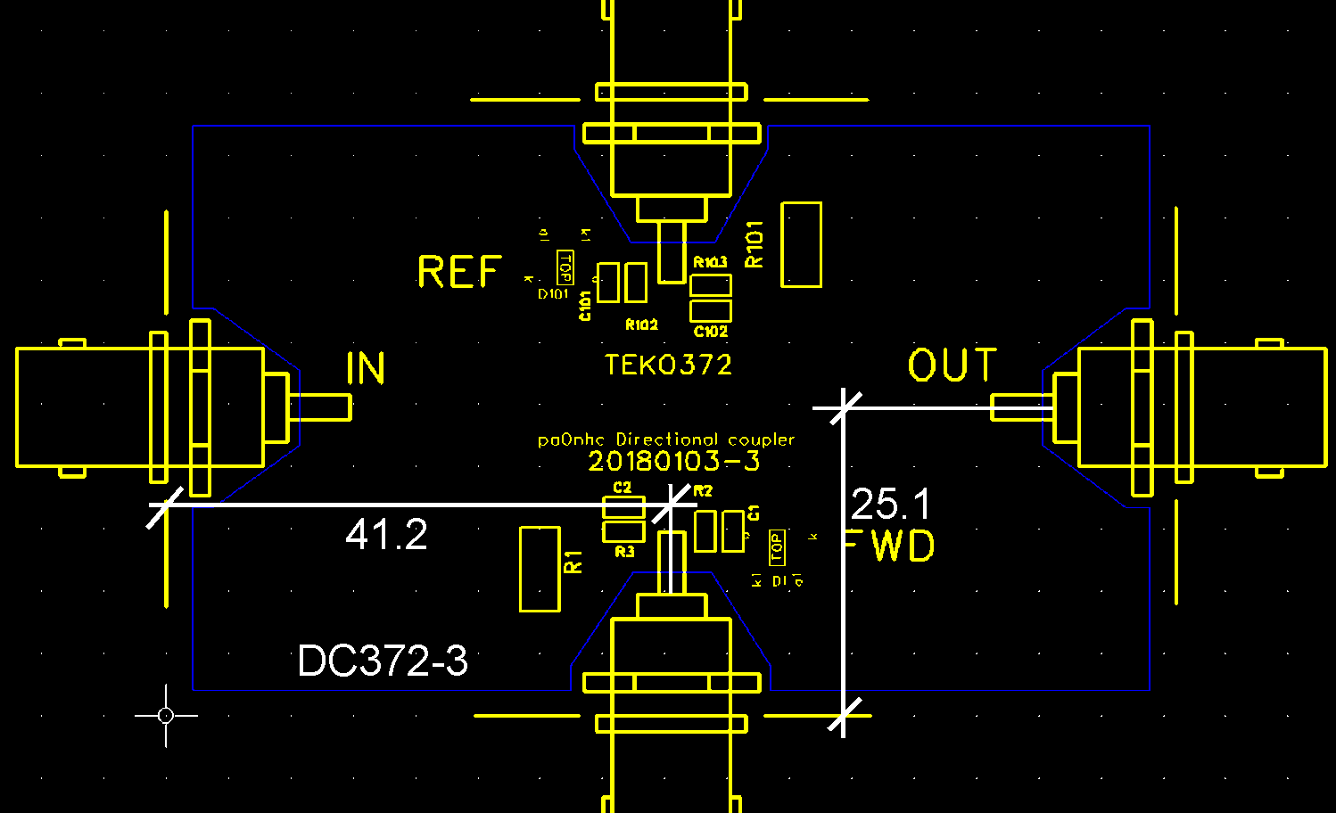
The enclosures are TEKO type 371 or type 372. Which one is printed onto the PCB
top silk.
The BNC busses are short
types (for max. 3.5mm wall thickness), with nut, lock ring, PTFE
(Teflon (R)) insulation and each two long grounding lugs. For mechanical
and electrical stability, their rim should be soldered directly onto the outside
of the box.
All parts numbers are printed onto the top surface of the PCBs.
R1/101 are size 2010 50 Ohms 1% 2W or two 100 Ohms
1% 1W soldered on top of each other (parallel).
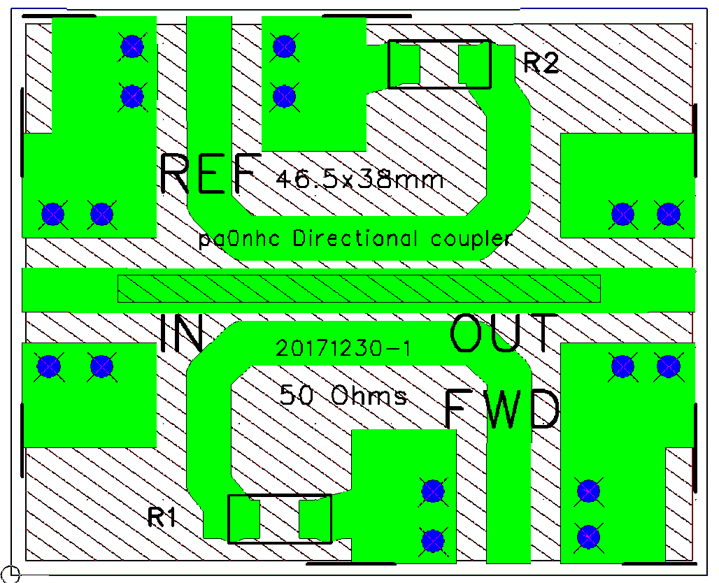
Details of the PCBs.
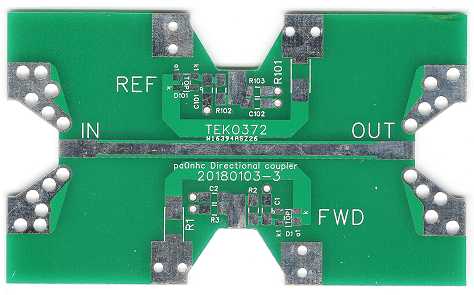
Four, especially shaped PCBs, will fit with 0.5mm free space inside RF-tight TEKO 371 or 372 1mm steel enclosures.
Connections are four short length BNC busses (for max wall
thickness 3.5 mm) with PTFE (Teflon (R))
insulation, nut mount, and each
with two long ground lugs.
These PTFE BNC busses can best be soldered onto the outside of the TEKO
boxes. Nuts an rings are discarded.
The two small PCBs without BNC busses are designed to be installed inside equipment, with coaxes soldered to the PCB. It is wise to wind a few windings of each coax through a Fair-Rite mix #31 core to block common mode currents.
The bottom copper of the PCBs is full mass plane. A number of carefully placed wide-hole-vias ensure good RF inter connections between top and bottom ground surfaces.
The
PCB mass planes must only
be connected to the mass of the BNC busses via two ground lugs at each BNC bus.
If the current capacity of the through line track need to be improved, it can
be filled with a thicker layer of solder tin. They intentionally are partly kept
free from solder mask.
Each terminating resistor is one SMD resistor 50 Ohms 1% 2W size 2010, or two 100 Ohm 1W size 2010 SMD resistors in parallel, soldered on top of each other (totally 50 Ohms 2W).
On all PCB's, all component designators are printed. Just solder there the components from the parts list.
The detector diode is a Skottky UHF type, with very low threshold voltage, if loaded with 100 kOhms or higher value.
If available, use a BAT62 (single diode, white stripe = k).
A double
diode version of it BAT62-03W can also be used (one diode is not
connected).
The PCB shows where the wide leg (anode) should be
located. See picture
==> .
Properties.
These RF couplers are usable between 28 MHz and 435 MHz, and designed to have
abt. -32dB @ 145 MHz output (32dB coupling loss) in respect to its main 50 Ohms thru-line.
The value of their coupling loss rises 6dB / octave
towards lower frequencies, and vice versa.
The 50 Ohms terminating resistors on the PCBs will dissipate
1W heath when 7,07Vrms is induced into them.
Solder a 50 Ohms 2W resistor or two 1W 100 Ohm resistors in parallel (on top of
each other).
REM : For more than 100W input, i suggest to fill the tinned part of the through-line
with a thick layer of solder.
On 145 MHz the coupling loss is ca. 32dB (1/1000
power). The maximal power input on 145 MHz is 1.5kW.
On 435 MHz, the coupling loss is 10dB less, ca. 22 dB (1/100 power). The
maximal power input on 435 MHz is 150W.
On 29 MHz the coupling loss is 5 times higher (ca. 46dB). With 1kW input abt. 1.4Vrms is induced into the coupling lines.
If such couplers should be used below 29 MHz, the coupling loss becomes to high, making it useless for use on short wave bands lower than 29 MHz.
Drawings for drilling
holes in the TEKO boxes.
Dimensions in millimeters.
Drill the BNC holes at a distance of 10mm from the bottom.
See also assembling instructions at the top of this page.
 PCB-RF-371 Small coupler with RF output. 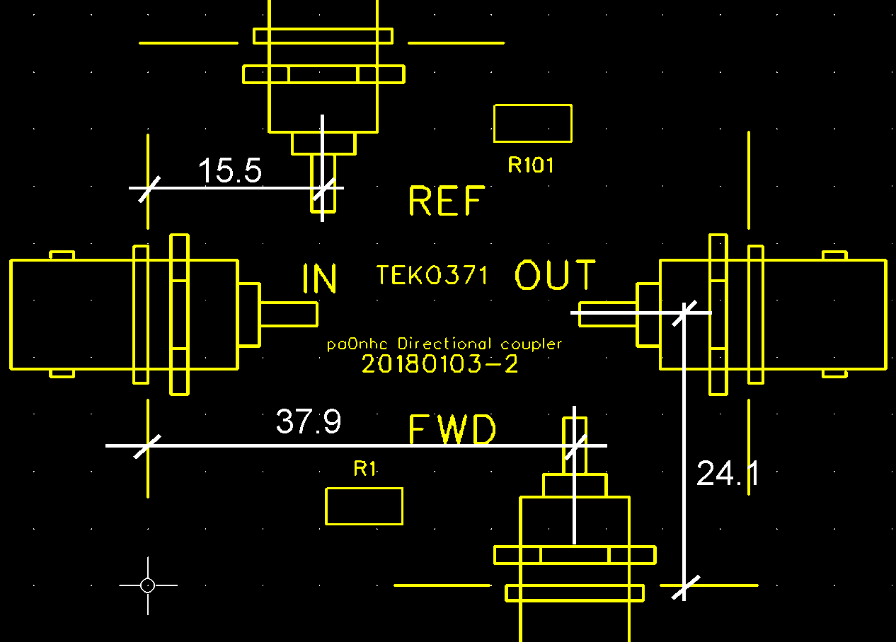
|
|
|
|
|
|
|