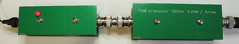
0dBm generator + fixed 63dB attenuator. Output S9 +- 0.2dB.
Total dimensions 9x3.5 x 2.4 cm3
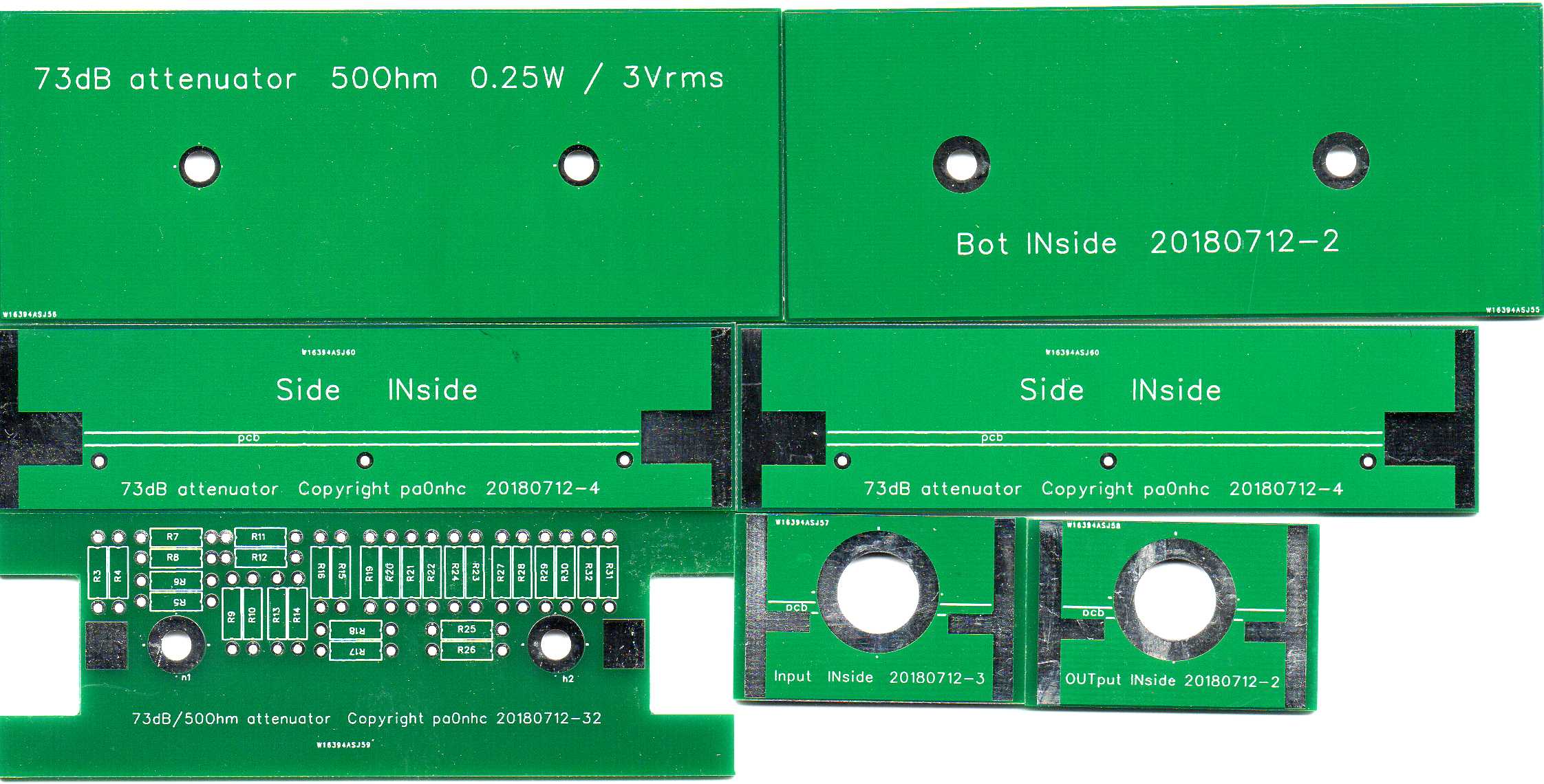
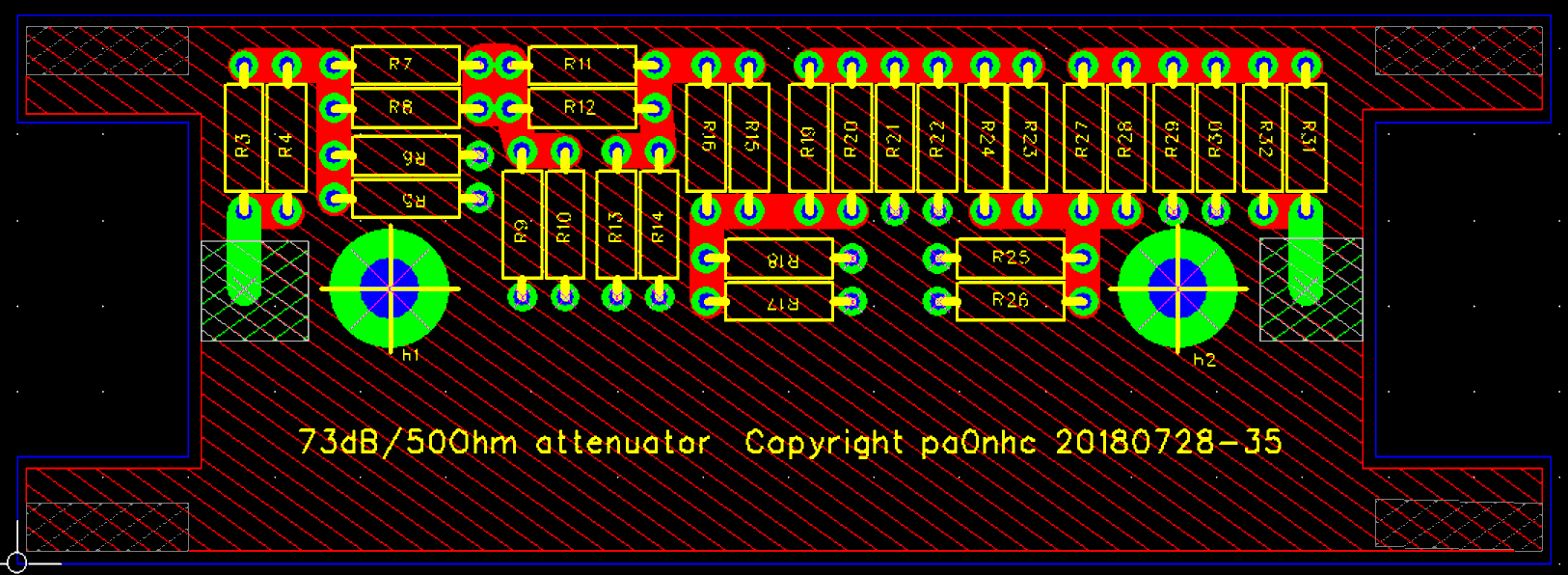
Rem ; the "73"on the PCB parts text is wrong. Sorry. It should be "63".
| << |
pa0nhc fixed 63dB 50 Ohm attenuator 20180829 / 20181210 / 20200820 |
Copyright.
The use, copy and modification of all info on this site is only permitted for non-commercial
purposes, and
thereby explicitly stating my radio amateur call sign "PA0NHC" as the
original writer / designer / photographer / publisher.
Nominal in- and output impedances : 50 +/- 0.2 Ohm.
Nominal attenuation : 63 +/- 0.2 dB.
Max input : 0.25W / 3.5 Vrms.
Intended use :
Calibrating receiver S-meters to S9+10 dB, by using a 0dBm signal generator
as signal source.
With an extra step
attenuator the full range of the S-meter can be
calibrated.
0dBm generator + fixed 63dB attenuator. Output S9 +- 0.2dB.
Total dimensions 9x3.5 x 2.4 cm3
Rem ; the "73"on the PCB parts text is wrong. Sorry. It should be
"63".
The PCB set is available.
|
||||||||||||||||||||||||||||||||||||||||||||||||||||||||||||||||||||||||||||||||||||||||||||||||||||
According to IARU :
Short Wave : S9 = 50 uV (-73dBm), 1 s-point = 6 dB (2x received voltage
difference).
VHF : S9 = 5uV (-93dBm).
Japanese equipment :
often have S-meters which are indicating differently :
1 s-point = 3dB (2x transmitted power difference).
The total package consists of seven little double
sided PCBs.
The main PCB contains the attenuator circuit.
The other six PCBs are for the construction of a cheap, but neat enclosure. Already
painted.
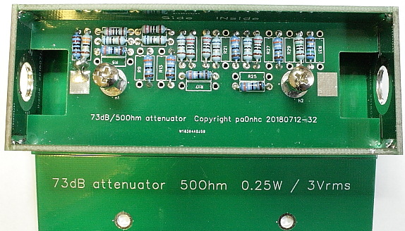
The attenuator circuit consist or 5 stages.
All stages are of the "PI" type, and are connected in series. Fairly
accurate results are achieved, by using standard value resistors, connected in parallel. Easy soldering is ensured by using axial wired, 2.5x6.5mm 0.25W metal film resistors, and
RM8.6 / 1mm PCB holes.
A full PCB "ground" plane ensures a low inductance ground path, and small parasitic
capacitances between each resistor and "ground". This compensates a
little for the self
inductance of the used resistors, with the
goal to achieve a wider frequency range.
Construction.
The PCBs have solder masks which also serve as
outside lacquering.
On places where the PCB parts should be soldered together, tinned strips are
visible.
Correct positions are marked with lines.
See to it, that PCBs have 90 degr. angles in respect to each other.
When soldering panels together, at first just tack-solder each panel in
place, so you can correct its position.
In other words: start using two small solder point at one panel side with little
solder.
Only when all parts fit correctly, you can solder all seems fully.
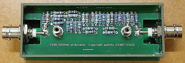
See the photos.
Start with soldering all resistors.
Tack solder the circuit PCB onto one long side.
Tack solder both small end panels
Tack solder the other long side panel.
Check that the lids will fit nicely.
Fill the seems with tin solder and flow nicely.
Install the BNCs, and solder its rim at one point
to the outside to the board. This locks the BNC in place and makes tightening
the nut easy.
Solder the pins.
You can first check the attenuation with DC
input.
Connect 3.0 Vdc via a series resistor of 50 Ohms to the attenuator input
Connect a load resistor of 50 Ohms to the attenuator output.
The output should be 2.12 mVdc.